Search
What is E-TEST? Flying Probe vs Tooling Test
- May 24,2024
-
Share
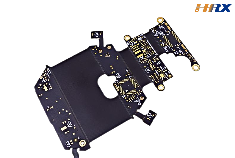
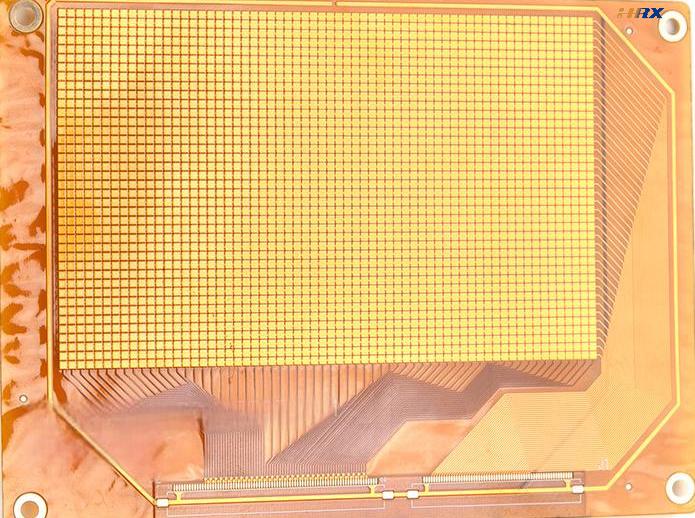
Before a bare FPC or PCB is delivered to the customer, it undergoes rigorous testing to ensure that it meets the required quality standards. One of the most critical tests in this process is the Electrical Test (E-Test). This test is essential for detecting any electrical faults, such as open circuits and short circuits, that could compromise the functionality of the final product.
This blog post will explore how PCB manufacturers use E-Test methods, including Flying Probe Testing and Tooling Testing, to ensure that each PCB meets the client’s specifications and functions correctly.
The Importance of E-Test
The primary purpose of the E-Test is to verify the electrical integrity of the PCB. Even though the board may look visually perfect, there could be hidden defects in the circuit pathways that could cause the board to malfunction in the final application. The two critical issues that E-Testing aims to identify are:
1. Open Circuits: These occur when the electrical path is incomplete, preventing current from flowing as intended.
2. Short Circuits: This happens when two conductive paths that should not be connected are bridged, causing unintended electrical flow that can damage components or cause system failure.
By catching these defects during the E-Test stage, manufacturers can prevent faulty PCBs from reaching the client, thus ensuring reliability and performance.

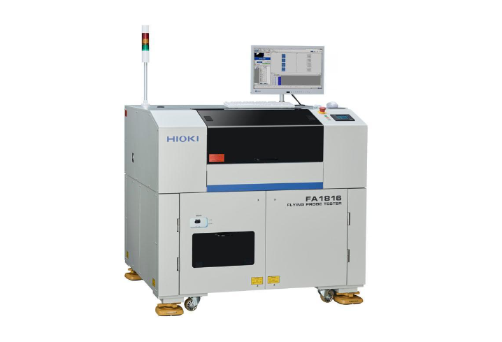
Flying Probe Test: Ideal for Sample Production
During the initial phases of a project, such as sample production or the pilot phase, manufacturers often use the Flying Probe Test for E-Testing. This method is slower compared to other testing methods, but it offers several advantages for small production runs and prototype testing:
No Need for Specialized Tooling: The flying probe test doesn't require dedicated fixtures or tooling. Instead, a set of robotic probes moves across the surface of the PCB, testing each connection point. This flexibility makes it ideal for projects that are still in the testing or prototype phase, where design changes are frequent.
Adaptability to Changes: Since no fixed tooling is required, design changes can be easily accommodated without the need to produce new test fixtures, saving both time and cost.
Time-Consuming but Precise: Although the flying probe test is slower, it is highly accurate in detecting faults on complex boards. Each probe moves independently, allowing it to test a wide variety of net patterns and layouts.
For smaller batches or prototype testing, where the emphasis is on precision rather than speed, the flying probe test is the go-to method for ensuring electrical integrity.

Tooling Test: Essential for Mass Production
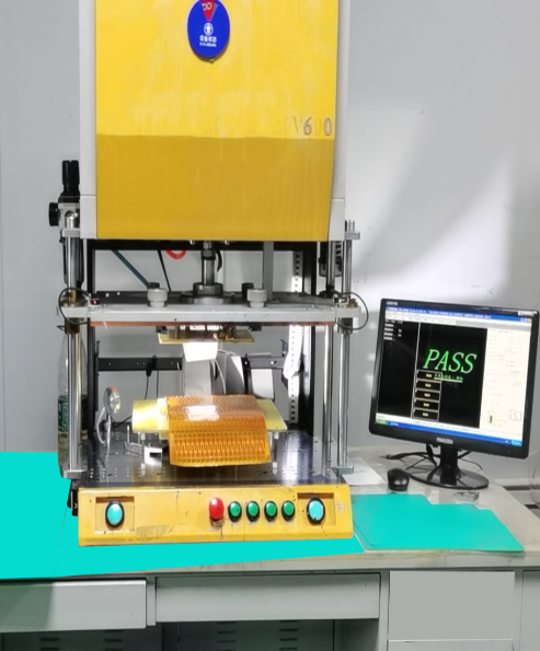
As a project moves from sample production to mass production, the demands on testing efficiency increase. In this stage, PCB manufacturers typically shift to using Tooling Testing, also known as a bed-of-nails test, for E-Testing. This method involves creating specialized fixtures or tooling designed specifically for the PCB project.
Faster Testing: Unlike the flying probe test, which sequentially checks each connection, tooling tests use a bed of fixed probes to simultaneously test all critical points on the PCB. This reduces testing time significantly, making it ideal for high-volume production.
Dedicated Fixtures: To conduct tooling tests, manufacturers create custom fixtures that match the specific design of the PCB. While creating these fixtures requires an initial investment of time and resources, it pays off in the speed and efficiency it brings to the testing process once mass production is underway.
Detecting NG Circuits: Just like the flying probe test, tooling tests are designed to detect any NG (No Good) circuits, including open and short circuits. The main difference is that tooling tests do so at a much faster pace, making them more suitable for large-scale production environments.
Ensuring Quality Through E-Test
Whether using the Flying Probe Test for small batches or Tooling Test for mass production, the goal of E-Testing remains the same: to ensure that the bare PCB meets the client’s standards for quality and performance. By detecting and addressing any electrical faults before the PCB leaves the factory, manufacturers can provide their clients with reliable products that are ready for final assembly and use.
In conclusion, the E-Test is a crucial step in PCB manufacturing, designed to identify any electrical defects that could lead to product failures. During sample production, manufacturers rely on the Flying Probe Test for its flexibility and accuracy, even though it may be more time-consuming. As projects scale into mass production, the Tooling Test becomes the preferred method for its speed and efficiency.
By incorporating these E-Testing methods, PCB manufacturers can ensure that their products meet the highest standards of quality and reliability, providing clients with confidence in the final product’s performance.

Let’s talk! We’ll provide the perfect solution for you!
-
 Huaruixin Electronics mainly produces printed circuit boards as the core business, to provide customers with one-stop solutions for FPC/PCB production, components sourcing and Assembly.
 - WHAT WE DO — PCB Design Solutions — Flex PCB Production — Components Sourcing — FPC&PCB Assembly
- PRODUCTS — Single Sided Flexible Circuits — Double Sided Flexible Circuits — Multilayer Flexible Cirucits — Rigid-Flex Circuits — FPC Assembly — PCB Assembly
- CAPABILITY — FPC Capability — Rigid-Flex Capability — PCB Capability — Assembly Capability
- Copyright © 2024 Shenzhen Huaruixin Electronics Co., Ltd. All Rights Reserved.
- Design By BONTOP


