Search
Understanding Gold Surface Area Calculation on PCBs and Its Impact on Pricing
- Oct 07,2024
-
Share
PCBs or FPCs are the backbone of almost all electronic devices, ensuring that electrical signals move effectively between components. One of the key considerations during PCB manufacturing is the surface finish, and one of the most valuable materials used is gold, typically applied through Electroless Nickel Immersion Gold (ENIG) coating. While gold enhances conductivity and durability, it also comes with higher costs. This blog will address common questions about how gold surface area on a PCB is calculated and why it affects pricing.
What is Gold Surface Area on a PCB?
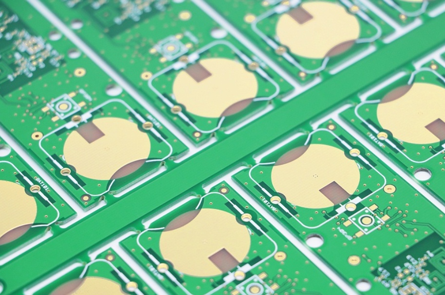
Gold surface area refers to the portion of a PCB’s surface that is covered with a thin layer of gold, usually for enhanced conductivity, durability, and corrosion resistance. Gold is primarily used in areas where the PCB will be subject to frequent mechanical wear, such as connector pads, edge fingers, and component pads. It ensures reliable long-term electrical performance, making it an essential choice for high-performance or mission-critical devices.
However, because gold is expensive, its usage must be optimized, which brings us to the question of how gold surface area is calculated and how it impacts the overall cost of the PCB.

How to Calculate Gold Surface Area
Calculating the gold surface area is a relatively straightforward process. It involves determining the total area of the PCB that is coated with gold. Here’s a simple formula:
Gold Surface Area (mm²) = Sum of the surface area of all gold-plated regions on the PCB.
To calculate this, you need to measure the dimensions of all the gold-coated sections (such as pads, traces, or connectors) and sum them. Modern PCB design software can automate this process, providing the exact gold surface area once the design is complete.
Example:
Let’s say a PCB has gold plating over two rectangular connector pads, each measuring 4mm x 2mm. The total gold area for each pad would be:
4mm x 2mm = 8mm²
If there are two such pads, the total gold surface area would be:
2 x 8mm² = 16mm²
Default Gold Surface Area and Free Coverage Limits
Manufacturers typically allow a certain percentage of the PCB's total surface area to be coated with gold without incurring additional costs. This is known as the "default gold surface area" and can vary by manufacturer, but it generally ranges between 5% to 10% of the total PCB area.
For example, if your PCB has a total surface area of 1000mm², up to 100mm² of gold plating may be included at no extra charge. However, if the gold-plated area exceeds this threshold, additional costs will be incurred.
Why Does the Price Increase with Gold Surface Area?
Several factors contribute to the higher costs when the gold surface area increases:
1. Material Costs: Gold is a precious metal, and its price fluctuates based on global markets. More surface area covered with gold directly increases the cost of the raw materials needed for the board.
2. Manufacturing Complexity: Applying gold plating to large or intricate areas requires more careful processing, which increases the production time and complexity. Complex designs with irregular gold areas may also require more detailed masking and application techniques.
3. Waste Management: The process of applying gold often involves chemical solutions. The more gold that is applied, the more solution is needed, and managing or recycling unused gold adds to the overall cost.
How to Optimize Gold Usage on PCBs
As a PCB designer, it’s crucial to balance performance with cost-efficiency. Here are some strategies to help optimize gold usage:
Use Gold Sparingly: Only apply gold where absolutely necessary, such as on critical connectors or high-wear areas.
Alternative Finishes: In some cases, using other surface finishes like HASL (Hot Air Solder Leveling) or OSP (Organic Solderability Preservative) may provide cost savings, though they may not offer the same performance as gold.
Collaborate with Your Manufacturer: Work closely with your PCB manufacturer to understand their gold surface area thresholds and any options for optimizing the design to stay within these limits.
Conclusion
Gold surface area on a PCB is a critical factor that affects both the performance and cost of the board. By understanding how to calculate gold surface area, knowing industry standards for free coverage, and implementing smart design strategies, you can optimize the use of gold in your PCB designs. Keeping a balance between gold usage and cost is key to ensuring that you get the performance you need without exceeding budget constraints.
By being mindful of these factors, PCB designers can make informed decisions that lead to high-quality, cost-effective products.

Let’s talk! We’ll provide the perfect solution for you!
-
 Huaruixin Electronics mainly produces printed circuit boards as the core business, to provide customers with one-stop solutions for FPC/PCB production, components sourcing and Assembly.
 - WHAT WE DO — PCB Design Solutions — Flex PCB Production — Components Sourcing — FPC&PCB Assembly
- PRODUCTS — Single Sided Flexible Circuits — Double Sided Flexible Circuits — Multilayer Flexible Cirucits — Rigid-Flex Circuits — FPC Assembly — PCB Assembly
- CAPABILITY — FPC Capability — Rigid-Flex Capability — PCB Capability — Assembly Capability
- Copyright © 2024 Shenzhen Huaruixin Electronics Co., Ltd. All Rights Reserved.
- Design By BONTOP


