PCB Welding Optimization: Minimizing Warping Deformation
- Nov 25,2024
-
Share
In the realm of PCB manufacturing, welding large copper bars onto the board is a crucial yet challenging process. The disparity in thermal expansion coefficients between copper and the surrounding PCB materials, such as glass fiber reinforced substrates, often leads to warping or deformation of the PCB. This occurs due to the uneven heat distribution during welding, causing local thermal expansion and contraction, which in turn generates mechanical stress.
Consequences of PCB Warping Deformation
When a PCB warps, it can have several detrimental effects. Circuit connection failures are common, as the deformation disrupts the proper connection between electronic components, potentially leading to breaks or short circuits. This can render the entire circuit inoperative. In high-frequency or high-precision circuits, performance loss is also a significant concern. The warped board may result in signal transmission loss, increased noise, or signal distortion. Additionally, the mechanical stability of the PCB declines, making it difficult to install within a device and affecting the overall stability and performance of the equipment. Long-term reliability is compromised as stress concentrations develop, shortening the PCB's lifespan and increasing the risk of failure. Severe warping also poses maintenance difficulties, often requiring complex repair procedures or complete board replacement, which escalates repair costs and time.
Factors Leading to PCB Warping after Welding Large Copper Bars
Thermal Expansion Coefficient Difference: Copper has a relatively high coefficient of thermal expansion compared to the PCB substrate. During welding, the copper bar expands more rapidly, and upon cooling, the differential contraction causes mechanical stress and warping.
Thermal Stress: The high temperatures during welding induce local thermal expansion. When the board cools, the varying temperature change rates across different areas create thermal stress, which can cause the board to bend.
Plate Design and Thickness: A thin PCB or a design that fails to account for the impact of large copper bars is more prone to warping. Insufficient consideration of the mechanical forces during the design stage can increase the deformation risk.
Improper Welding Temperature and Process Control: Excessive or uneven welding temperatures can lead to local overheating of the board, causing the material around the copper bar to expand and deform.

Solutions and Design Considerations
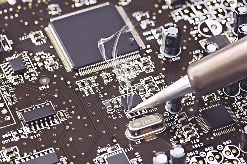
Optimize Welding Process: Precise control of welding temperature and time is essential. For example, using a temperature-controlled soldering iron or a reflow soldering oven with accurate temperature profiles can ensure uniform heat distribution. Employing techniques like wave soldering with proper flux and solder alloy selection can also help. In a recent project at Shenzhen Huaruixin Electronics Co., Ltd., by carefully adjusting the reflow profile and using a high-quality solder paste, the temperature variation across the PCB was reduced to within ±2°C, significantly minimizing warping.
Design Suitable Support Structures: Incorporating support structures near large copper bars or reducing the copper bar area in the layout can mitigate warping. For instance, adding small metal braces or vias in strategic locations can distribute the thermal expansion forces. A customer of Shenzhen Huaruixin Electronics Co., Ltd. redesigned their PCB layout to include additional support vias around a large copper power plane. This simple modification reduced the warping by over 50% compared to the previous design.
Increase Sheet Thickness or Strengthen Support: A thicker PCB can better withstand thermal stress. Alternatively, reinforcing the support around the large copper bar, such as using a stiffer substrate material or adding extra layers of fiberglass, can enhance rigidity. Shenzhen Huaruixin Electronics Co., Ltd. has successfully produced thicker PCBs with enhanced copper bar support for a high-power electronics application, ensuring minimal deformation even under extreme thermal cycling.
Material and Structure Optimization: Selecting materials with lower thermal expansion coefficients, like some specialty polymers or composites, can reduce the differential expansion issue. Moreover, optimizing the board structure during the design phase, such as using a symmetrical layout or adding stress relief features, can further prevent warping. In a particular design for a sensitive communication device, Shenzhen Huaruixin Electronics Co., Ltd. used a hybrid substrate with a low CTE core and copper-clad layers, combined with a carefully designed symmetrical layout. This approach eliminated visible warping and maintained excellent signal integrity.
Temperature Control and Cooling Process: Implementing a gradual cooling process after welding is crucial. This can be achieved using cooling fans with adjustable speed or a water-cooled heat sink in contact with the PCB. Shenzhen Huaruixin Electronics Co., Ltd. has developed a custom cooling fixture that allows for controlled cooling rates, preventing rapid temperature changes that could lead to warping.
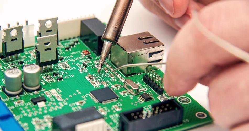
Using Auxiliary Tools: Temporary support tools like clamps or jigs can be used during welding and cooling to maintain the flatness of the copper bar and the PCB. These tools can be easily removed after the process is complete. In a mass production line at Shenzhen Huaruixin Electronics Co., Ltd., custom-designed clamps were used during the soldering of large copper bars, ensuring consistent flatness and reducing the rejection rate due to warping to less than 1%.
In conclusion, as design engineers, we must consider all these factors and implement the appropriate solutions to minimize PCB warping deformation during and after the welding of large copper bars.
Shenzhen Huaruixin Electronics Co., Ltd., with its extensive experience in PCB&FPC production and sales, is always ready to collaborate with customers and industry peers to further enhance the quality and reliability of PCB designs.


 Huaruixin Electronics mainly produces printed circuit boards as the core business, to provide customers with one-stop solutions for FPC/PCB production, components sourcing and Assembly.
