Search
Deciphering the Intricate Tapestry of FPC Production and Design Process
- Jan 02,2025
-
Share
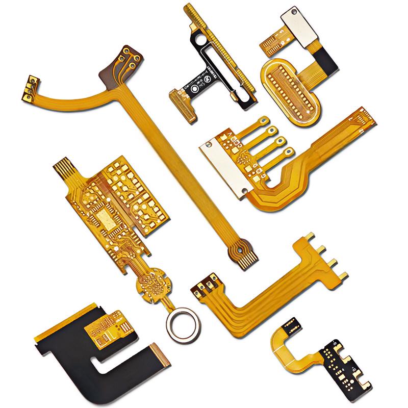
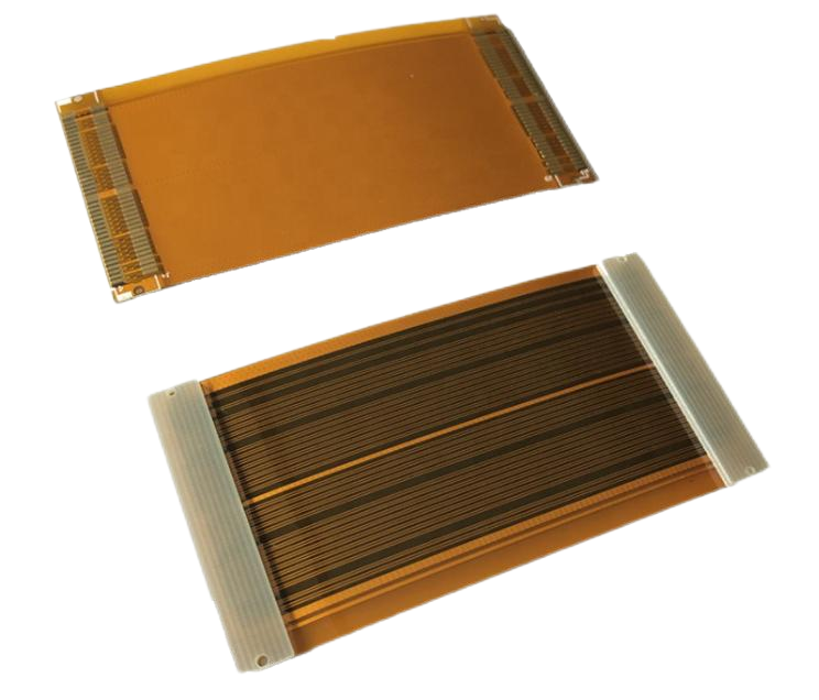
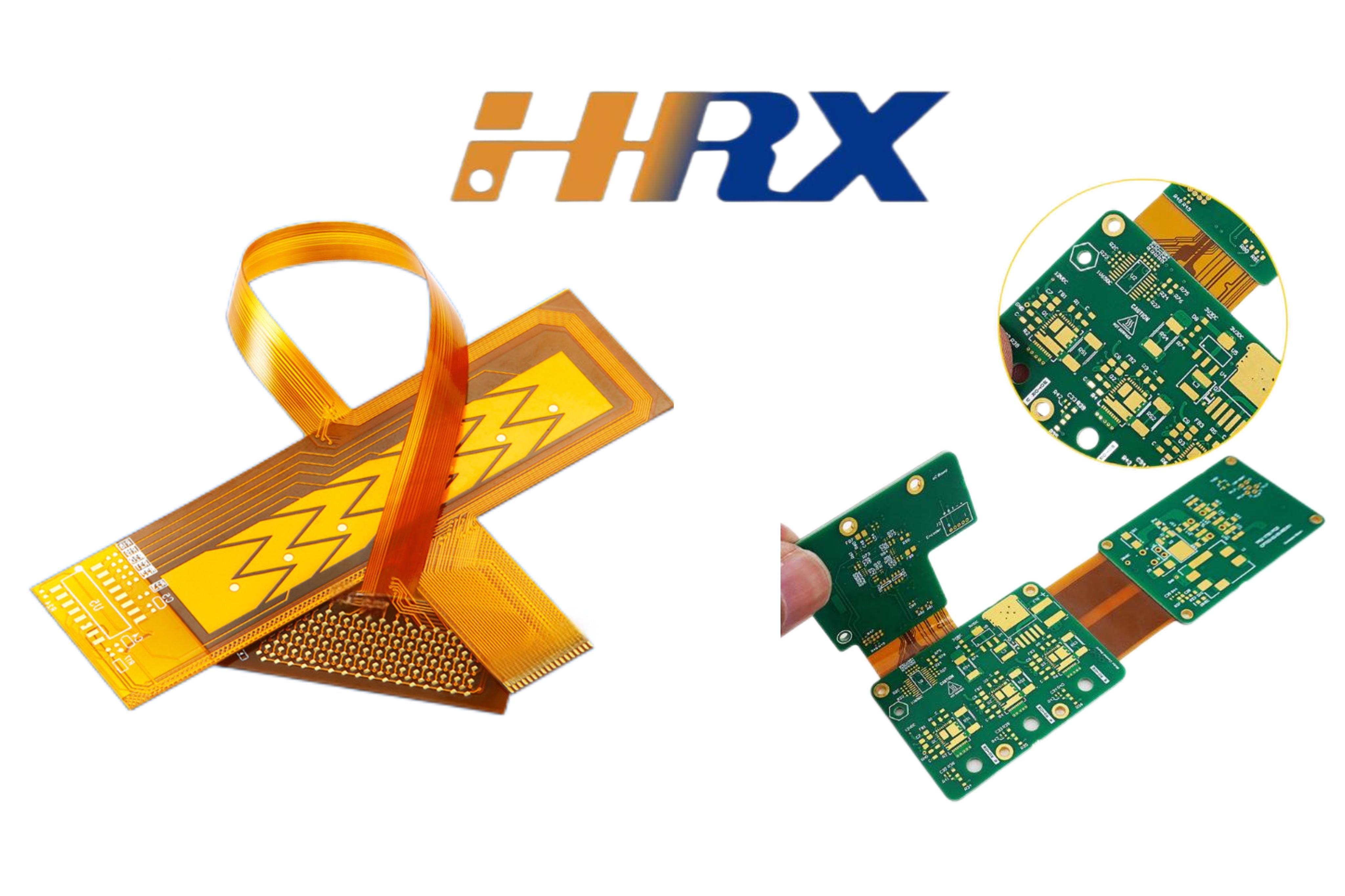
In the vibrant and ever-evolving panorama of the electronics universe, Flexible Printed Circuits (FPCs) have emerged as a linchpin technology, providing the essential foundation for the streamlined functionality and seamless amalgamation of modern-day electronic devices. Today, we are about to embark on an elaborate expedition through the highly convoluted and meticulously refined production and design odyssey of FPCs.

1.Inception of Design and Preliminary Reconnaissance
The genesis of an FPC design project initiates with a painstaking deconstruction and lucid explication of the design prerequisites. This necessitates immersive and highly detailed dialogues with clients, delving deep into the minutiae to precisely ascertain the exacting functionality and performance benchmarks that the FPC must achieve. Consider, for example, an FPC earmarked for a state-of-the-art smartphone application. In such a scenario, it becomes of utmost importance to determine whether its raison d'être is to establish connections between the camera module, the display panel, or other integral components. Moreover, minute details regarding signal transmission velocity, power dissipation thresholds, impedance characteristics, and even the critical crosstalk attenuation imperatives are meticulously charted and analyzed. Equally crucial is a comprehensive understanding of the FPC's operational environment, spanning temperature gradients, humidity spectra, and potential exposure to chemical agents. For an FPC slated for deployment in the vicinity of a vehicular engine, it must possess the robustness to withstand elevated temperatures, repel oil ingress, and endure mechanical vibrations without any compromise to its performance integrity.
Concomitantly, an exhaustive compilation of relevant data is set in motion. This encompasses the procurement of precise mechanical dimensions and interface protocols of the end-product. In cases where the FPC is envisioned as a retrofit solution for an existing device, painstaking efforts are expended to extract and assimilate details such as the original board's physical dimensions, pin configurations, and signal routing schematics. In parallel, unwavering adherence to industry-sanctioned standards and specifications, epitomized by the IPC - 2223 guidelines governing flexible printed board design, is ensured. This not only fortifies the technical soundness of the design but also facilitates seamless interoperability and manufacturability, aligning with the best practices of the FPC fraternity.
2.Schematic Engineering and Component Conception
The circuit function design phase witnesses the adept utilization of industry-leading electronic design software suites, such as Altium Designer or Cadence Allegro. Here, the circuit schematic takes shape, with each component - be it microcontrollers, resistors, capacitors, or inductors - meticulously interconnected to actualize the envisioned functionality. Signal integrity reigns supreme, especially in the context of high-speed digital and analog signal pathways. Sophisticated techniques like differential pair routing, impedance matching, and ground plane isolation are judiciously deployed to curtail electromagnetic interference (EMI) and safeguard signal fidelity, thereby ensuring error-free data transmission and reception.
Subsequent to this, the process of component selection unfolds. Each component is painstakingly handpicked, with due consideration given to its performance metrics and compatibility with the overall design. When zeroing in on a microcontroller, for instance, factors such as processing power, clock speed, power dissipation profiles, and available peripherals are meticulously evaluated. For passive components, parameters like tolerance levels, voltage ratings, temperature coefficients, and frequency responses are scrutinized. Additionally, the packaging form factor of each component is meticulously vetted to ensure seamless integration within the constraints of the FPC manufacturing process, which often demands compact and space-efficient designs, given the pliable nature of the substrate.
3.Layout Orchestration and Routing Mastery
The layout planning stage involves the strategic arrangement of components within the FPC's design canvas. This is a delicate ballet of space optimization and signal flow management, where components with related functions are clustered in close proximity. This not only truncates signal propagation delays but also mitigates the risk of crosstalk and EMI. Thoughtful consideration is also accorded to the FPC's physical contours and its intended mode of integration. Connectors, for example, are strategically positioned along the edges to ensure effortless mating and disconnection, while also factoring in the mechanical stress and strain during assembly and operation.
Routing design, the next critical step, adheres to a set of stringent and well-defined wiring protocols. High-priority signals, such as clock pulses and high-speed data streams, are accorded preferential treatment, with their paths meticulously planned to be as short and direct as possible. This is achieved through the judicious minimization of via counts, which can otherwise introduce signal reflections and impedance discontinuities. Power and ground planes are designed with ample width to accommodate the requisite current densities, thereby preventing voltage drops and ensuring stable power delivery. Adequate spacing between conductors is maintained to preclude short circuits and mitigate the risk of electromagnetic coupling. Given the pliable nature of FPCs, special care is taken to avert the congregation of wires in regions prone to bending, as this could precipitate wire fractures and compromise the circuit's integrity over time.
4.Design Scrutiny and Validation
An internal design review represents a critical checkpoint in the FPC design odyssey. The design team, armed with their collective expertise and a discerning eye, meticulously examines every facet of the circuit functionality, the rationality of the wiring topology, and the adherence to established design rules. The correctness of component footprints and their seamless alignment with the manufacturing process are also placed under the microscope. For example, the solder pad dimensions and geometries are meticulously verified to ensure optimal wetting and bonding during the soldering process, which is a critical determinant of the FPC's long-term reliability.
Following this, the design is presented to the client for their evaluation and feedback. This iterative process of client review and designer refinement is a crucible where the design is honed to perfection. The client may proffer suggestions or requisitions pertaining to alterations in the FPC's functionality, dimensional constraints, or connector placements, all of which are assimilated and translated into design modifications.
5.Production Artifact Generation
The creation of production files is a pivotal step that bridges the chasm between design and manufacturing. Gerber files, the lingua franca of the PCB manufacturing world, are meticulously exported from the design software. These files encapsulate the graphical representations of the circuit layers, the drill patterns, and other essential manufacturing details. Complementary files, such as drill files specifying the precise locations and diameters of holes, and solder mask files defining the areas to be protected during the soldering process, are also generated. This constellation of files provides the manufacturing facility with a comprehensive and unambiguous blueprint for bringing the FPC to life.
Accompanying these files is a detailed production instruction manual. This document is a compendium of technical specifications, delineating the FPC's material requisites, including the choice of substrate material, its thickness and flexibility characteristics, and the copper foil thickness and quality grade. It also spells out the exacting process parameters, such as the surface treatment modalities - be it electroless nickel immersion gold (ENIG), hot air solder leveling (HASL), or organic solderability preservative (OSP) - and the minimum allowable bending radius to ensure the FPC's mechanical durability. In cases where the FPC is destined for component assembly, detailed assembly instructions, encompassing the sequence of component placement, soldering temperature profiles, and reflow profiles, are provided.
6.Production and Fabrication Expedition
The FPC substrate manufacturing process kicks off with the precise cutting of the flexible substrate material to the specified dimensions. This is followed by a series of photolithographic and chemical etching processes that etch the conductive pathways onto the substrate. Using advanced lithography techniques, the circuit pattern is transferred with micron-level precision onto the copper foil layer, which is then selectively etched to remove the unwanted copper, leaving behind the intricate network of conductive traces that form the backbone of the FPC.
Surface treatment is the next critical step, where the FPC is subjected to processes like gold or tin plating to enhance the solderability and conductivity of the exposed copper surfaces. This not only facilitates the reliable attachment of components but also augments the long-term corrosion resistance of the circuit. Subsequently, the solder mask is carefully applied, coating the areas that are not intended for soldering and thereby preventing short circuits and solder bridges.
The FPC then undergoes the shaping and testing phase. Precision cutting and bending operations are carried out to mold the FPC into its final form, conforming to the exacting dimensional and mechanical requirements. Rigorous electrical testing regimens are then instituted, encompassing open/short circuit tests to detect any discontinuities or inadvertent connections, insulation resistance tests to ensure the integrity of the dielectric layers, and signal integrity tests to validate the performance of the high-speed signal paths. These tests are the litmus tests that determine the fitness of the FPC for its intended application.
7.Quality Assurance and Packaging Finale
Quality inspection is a multifaceted process that commences with a visual inspection of the FPC's surface. Any signs of scratches, blisters, or exposed copper are meticulously noted and evaluated for their potential impact on performance. The clarity and integrity of the circuit traces, as well as the quality of the component soldering joints, are also scrutinized under magnification. Dimensional measurements are taken with precision instruments to ensure strict compliance with the design specifications. Additionally, a battery of reliability tests, including high-low temperature cycling to simulate extreme environmental conditions, and bending life tests to gauge the FPC's mechanical endurance, are performed on a statistically significant sample size to ascertain its long-term performance and reliability.
Upon successful clearance of these quality benchmarks, the FPCs are carefully packaged using anti-static materials to safeguard them from electrostatic discharge, which can cause latent damage to the sensitive circuitry. Each package is meticulously labeled with essential product details, such as the model number, batch quantity, production date, and serial numbers, before being dispatched to the client, ready to be integrated into the next generation of electronic marvels.

For those seeking a paragon in the FPC manufacturing domain, Shenzhen Huaruixin Electronics Co., Ltd. emerges as a vanguard. Specializing in the production and distribution of FPCs, they have amassed a wealth of industry experience and expertise. Their state-of-the-art manufacturing facilities, manned by a team of seasoned professionals, are equipped to handle the most intricate FPC designs with finesse. Leveraging advanced manufacturing technologies and implementing stringent quality control protocols, they ensure that each FPC that rolls off their production line adheres to the highest standards of quality and performance. Whether you are a long-standing partner or a new entrant in the electronics arena, they extend a warm invitation to engage in fruitful exchanges and collaborations. Together, let's explore the boundless horizons of FPC technology and pioneer innovation in the electronics industry.

Let’s talk! We’ll provide the perfect solution for you!
-
 Huaruixin Electronics mainly produces printed circuit boards as the core business, to provide customers with one-stop solutions for FPC/PCB production, components sourcing and Assembly.
 - WHAT WE DO — PCB Design Solutions — Flex PCB Production — Components Sourcing — FPC&PCB Assembly
- PRODUCTS — Single Sided Flexible Circuits — Double Sided Flexible Circuits — Multilayer Flexible Cirucits — Rigid-Flex Circuits — FPC Assembly — PCB Assembly
- CAPABILITY — FPC Capability — Rigid-Flex Capability — PCB Capability — Assembly Capability
- Copyright © 2024 Shenzhen Huaruixin Electronics Co., Ltd. All Rights Reserved.
- Design By BONTOP


