Search
Deciphering the Intricacies of FPC Pad Design: Pitfalls and Proactive Solutions
- Jan 03,2025
-
Share
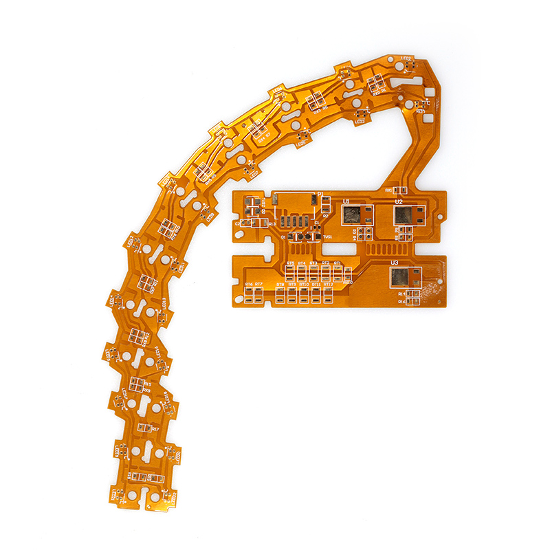
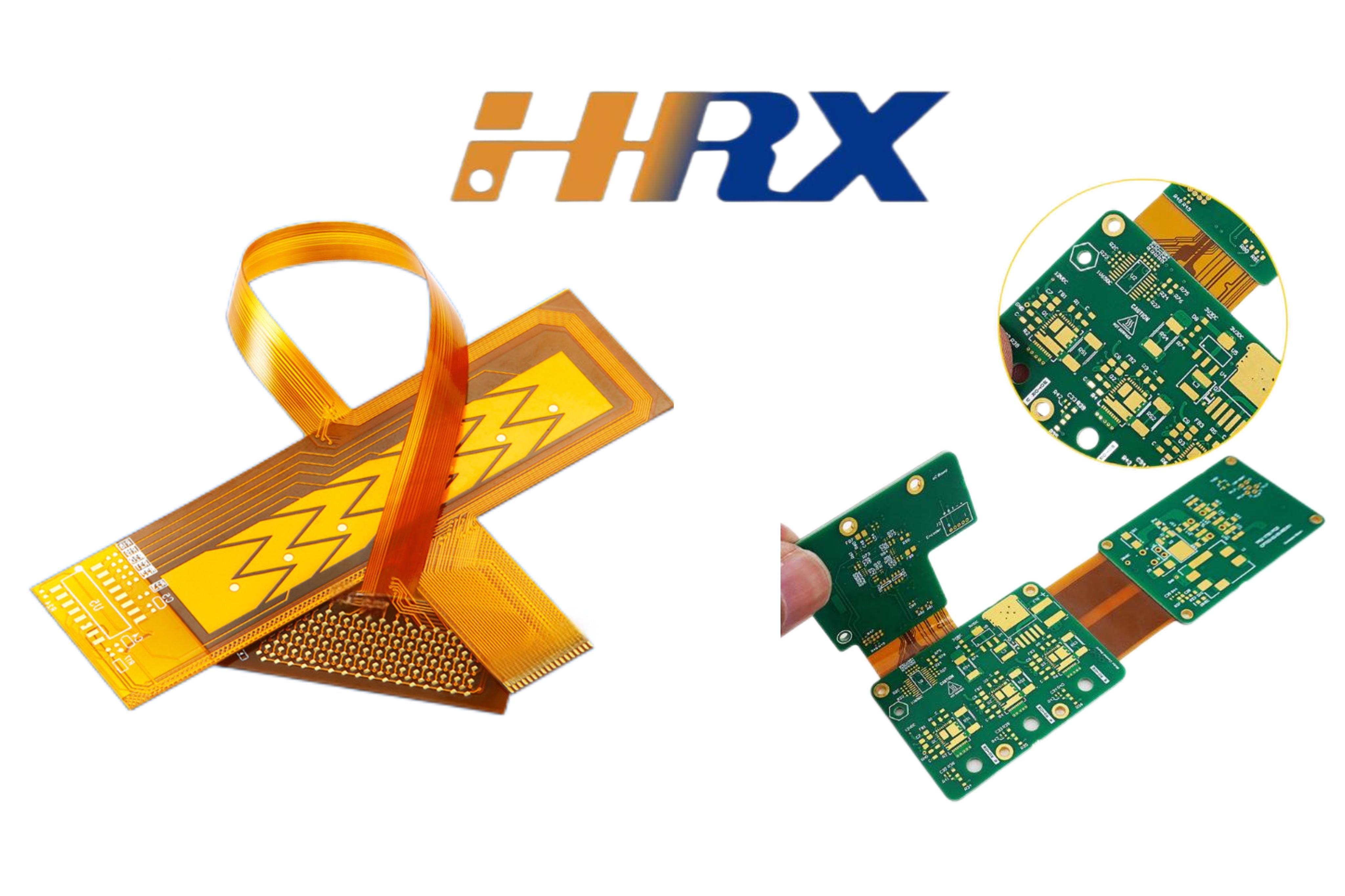
In the highly sophisticated domain of Flexible Printed Circuit (FPC) design, pad design emerges as a linchpin element that is often overlooked yet holds the key to the overall reliability and performance of the FPC assembly. In this technical exposé, we will plunge deep into the unique insights and nuances of FPC pad design, dissect the common stumbling blocks, and elucidate efficacious strategies to preemptively address them.

1. Unraveling the Paramount Importance of FPC Pad Design
FPC pads function as the vital nexus bridging the circuit traces and external components. They are obligated to furnish a stable, unwavering connection, facilitating seamless electrical conductivity while deftly withstanding mechanical stressors. In cutting-edge applications such as smartphones, wearable gadgets, and automotive electronics, where spatial constraints are stringent and flexibility reigns supreme, meticulously engineered pads are non-negotiable. Consider, for instance, an FPC in a smartwatch that interconnects the display module with the mainboard. Here, the pads must be artfully crafted to endure incessant bending, vibrations, and even potential torsional forces without compromising signal integrity, safeguarding the flawless operation of the device.
2. Distinctive Considerations in FPC Pad Design
a. Accommodating Flexural Dynamics
Given the inherently pliable nature of FPCs, pad designs must be astutely attuned to the exigencies of repeated bending and flexing. The pad geometry, encompassing shape and size, demands optimization to evenly distribute stress concentrations. Employing rounded corners on pads, as opposed to sharp ones, can substantially mitigate stress hotspots. This precautionary measure proves invaluable in thwarting pad cracking or delamination during the FPC's operational lifespan, which, in certain wearable applications, could entail thousands, if not tens of thousands, of bending cycles.
b. Navigating Spatial Constraints
In the compact cosmos of contemporary electronic devices, FPCs are invariably tasked with fitting snugly into minuscule spaces. Pad designers must adroitly balance the imperative for adequate pad area to ensure reliable soldering with the paucity of available real estate. This frequently necessitates inventive layout stratagems, such as implementing staggered pad arrangements or adopting miniaturized yet functionally robust pad geometries that scrupulously meet both electrical and mechanical requisites. In the context of a foldable phone FPC design, pads proximate to the folding hinge mandate painstaking sizing and precise positioning to avert interference while upholding seamless connectivity.
c. Preserving Signal Integrity
With the proliferation of high-speed signals in modern electronics, FPC pads must be architected to minimize signal reflections and impedance mismatches. This entails the deployment of techniques like controlled impedance pads, wherein the pad dimensions and the surrounding trace topology are meticulously calibrated to align with the characteristic impedance of the transmission line. In an FPC interfacing with a 5G module, any deviation from the optimal pad impedance could precipitate signal degradation, leading to data corruption and transmission errors.
3. Prevailing Problems in FPC Pad Design
a. Soldering Conundrums
Suboptimal solder wetting on pads represents a perennial affliction. This can stem from a gamut of factors, including improper pad surface finish, miscalculated pad size, or contamination. If the pad dimensions are too diminutive, there may not be sufficient area for the solder to form a tenacious bond, culminating in feeble connections. Conversely, if the surface finish is ill-suited for solder adhesion, such as a coarse or oxidized finish, solder balls may nucleate, or incomplete joints may materialize.
b. Pad Delamination
During thermal cycling or when subjected to mechanical stress, pads may succumb to delamination, detaching from the substrate. This is frequently attributable to inadequate adhesion between the pad and the underlying layer. Insufficient curing of adhesives during the manufacturing process or excessive stress concentration at the pad periphery can act as catalysts for this issue. Once a pad delaminates, it ruptures the electrical pathway, potentially precipitating device malfunction.
c. Signal Crosstalk
In multi-layer FPCs boasting closely spaced pads and traces, crosstalk between adjacent signals emerges as a significant tribulation. When pads are positioned too closely, the electromagnetic fields radiated by one signal can capacitively or inductively couple into an adjacent signal, thereby adulterating data. This quandary is particularly vexing in high-frequency applications such as radar systems or FPCs facilitating high-definition video transmission.
4. Tactical Approaches to Avert Problems
a. Precision-Engineered Pad Dimensions
Tailor the pad size with pinpoint accuracy based on the component type and soldering exigencies. For diminutive SMD components, adhere rigorously to the manufacturer's recommended pad dimensions, typically with a tolerance of ±0.05mm to guarantee proper solder wetting. For power components saddled with higher current demands, engineer wider pads to accommodate the augmented current density, with the width calibrated in accordance with industry benchmarks like IPC-7351.
b. Optimal Surface Treatment Selection
Choose the appropriate surface treatment for pads with sagacity. For general-purpose applications, electroless nickel immersion gold (ENIG) proffers a smooth, solderable surface that stoutly resists oxidation. In environments fraught with potential chemical exposure, such as automotive under-hood applications, organic solderability preservative (OSP) might be the more judicious choice. Institute regular monitoring and stringent control of the surface treatment process to uphold consistency.
c. Incorporating Stress Relief Mechanisms
Integrate stress relief architectures around pads. This could encompass adding fillets or chamfers to the pad edges to attenuate stress concentrations. In regions predisposed to bending, deploy flexible interconnects or compliant layers between the pad and the component to absorb mechanical stress. For example, in an FPC tethering a flexible sensor, a silicone-based compliant layer can act as a buffer, safeguarding pads during extreme bending episodes.
d. Meticulous Layout and Routing Protocols
Maintain a judicious spacing between pads and traces. A commonly adhered-to rule of thumb is to preserve a minimum spacing of 0.1mm between adjacent pads to curtail crosstalk. Route high-speed signals at a safe distance from sensitive pads and enlist shielding layers or ground planes to further insulate signals. In a complex FPC design underpinning a medical imaging device, meticulous layout planning can stave off signal interference, ensuring the accurate conveyance of diagnostic data.
5. Concluding Remarks
FPC pad design is a multifaceted discipline that demands unwavering attention to detail and a profound understanding of the underlying physics and engineering principles. By grasping the unique demands, anticipating potential pitfalls, and implementing sagacious solutions, designers can forge reliable and high-performing FPCs.
Shenzhen Huaruixin Electronics Co., Ltd., as a vanguard in the FPC manufacturing and distribution arena, armed with extensive industry acumen and expertise, stands ready to engage with fellow enthusiasts, be they new entrants or seasoned veterans. Whether you harbor queries regarding pad design, production methodologies, or quality control, we extend a warm invitation to reach out and explore the boundless frontiers of FPC technology in tandem. Let's coalesce our efforts to pioneer innovation and elevate the reliability benchmarks of flexible printed circuits.

Let’s talk! We’ll provide the perfect solution for you!
-
 Huaruixin Electronics mainly produces printed circuit boards as the core business, to provide customers with one-stop solutions for FPC/PCB production, components sourcing and Assembly.
 - WHAT WE DO — PCB Design Solutions — Flex PCB Production — Components Sourcing — FPC&PCB Assembly
- PRODUCTS — Single Sided Flexible Circuits — Double Sided Flexible Circuits — Multilayer Flexible Cirucits — Rigid-Flex Circuits — FPC Assembly — PCB Assembly
- CAPABILITY — FPC Capability — Rigid-Flex Capability — PCB Capability — Assembly Capability
- Copyright © 2024 Shenzhen Huaruixin Electronics Co., Ltd. All Rights Reserved.
- Design By BONTOP


