Search
Crucial Factors to Consider in the Design and Production of Flexible Printed Boards (FPBs)
- Feb 27,2025
-
Share
Material Selection
Base Film
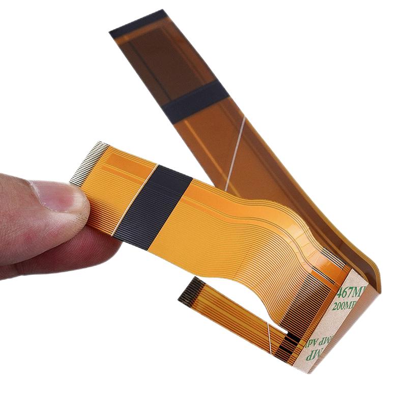
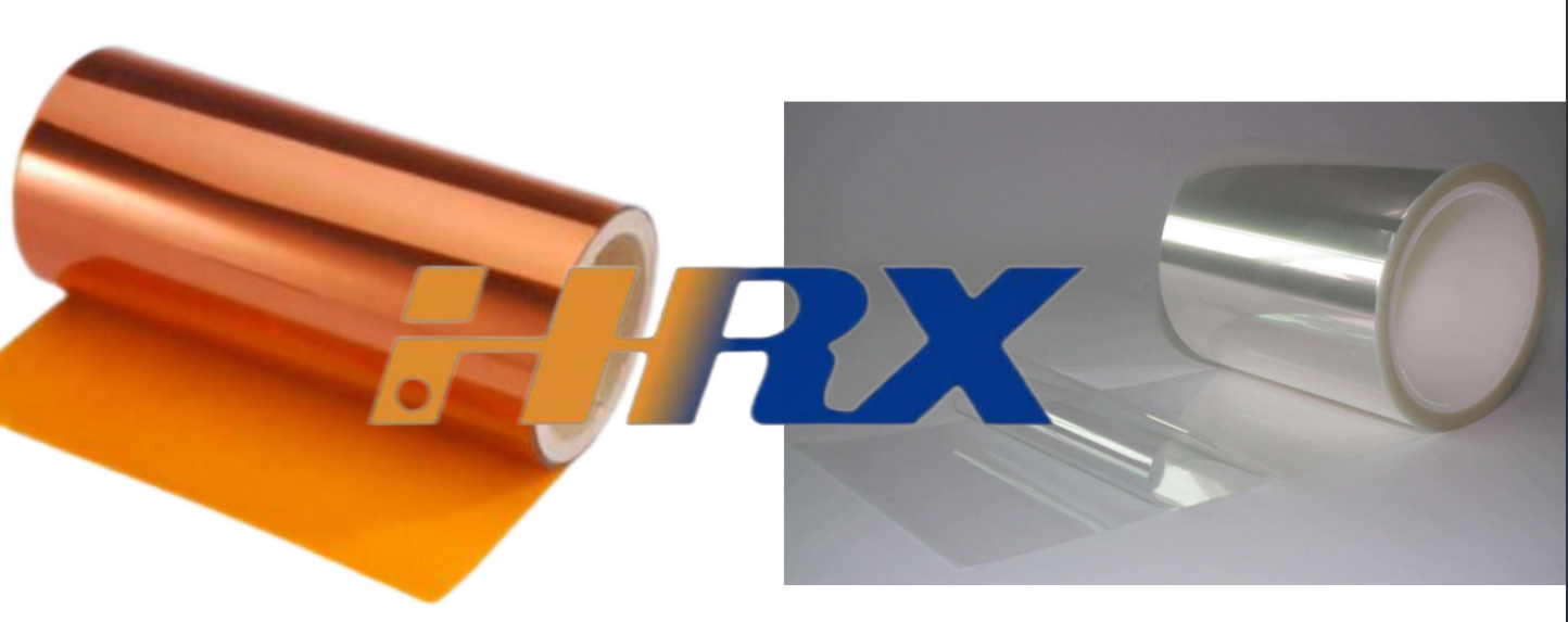
The selection of the base film is of utmost criticality. Polyimide (PI), renowned for its outstanding thermal resistance, chemical inertness, and mechanical robustness, is prevalently adopted. It is imperative to ensure that the thickness and quality of the base film align precisely with the requisites of the specific application scenario. For instance, in high - density interconnect (HDI) applications, a thinner base film might be indispensable to realize finer line widths and pitch, thus enhancing the circuit's miniaturization and performance density.
Adhesive
The adhesive employed for bonding disparate layers in FPBs must possess robust adhesion tenacity, pliability, and thermal resilience. In applications where gas emissions can detrimentally impact the end - product's performance, such as in aerospace or medical electronics, low - outgassing adhesives are highly preferable. These adhesives not only ensure stable bonding but also maintain a clean and contaminant - free environment within the device.
Copper Foil
The thickness of the copper foil exerts a profound influence on the current - carrying capacity and signal transmission fidelity. Thinner copper foils, with their reduced skin effect, are well - suited for high - frequency applications, where signal integrity is of paramount importance. Conversely, thicker copper foils are more appropriate for power - intensive circuits, capable of handling higher current loads. Additionally, the surface roughness of the copper foil, often characterized by the root - mean - square (RMS) value, should be carefully considered. A smoother surface can augment adhesion strength and mitigate signal attenuation, thereby optimizing the overall electrical performance.

Design
Line Width and Spacing
Engineer the minimum line width and spacing that the manufacturing process can feasibly accommodate while still satisfying the stringent electrical specifications. Narrower lines can augment the circuit density, but concomitantly, they may increase the resistance and capacitance, potentially compromising signal integrity. In high - speed digital circuits, for example, meticulous calculations of line width and spacing are essential to ensure that the high - frequency signals can be transmitted without distortion or attenuation. Signal integrity analysis tools, such as electromagnetic field solvers, are often employed to optimize these parameters.
Via Design
The dimensions and types of vias, including blind vias, buried vias, and through - vias, play a pivotal role in the FPB's performance. Blind and buried vias can significantly reduce the number of layers, leading to a more compact and efficient design. However, their manufacturing process is more intricate and requires advanced lithography and plating techniques. The aspect ratio, defined as the ratio of via depth to diameter, is a crucial parameter that must be carefully considered. A high aspect ratio can pose challenges in achieving complete via filling and reliable electrical connection, potentially leading to open - circuit failures.
Mechanical Design
Factor in the bending and flexing requirements of the FPB during the design phase. Design stress - relief features, such as rounded corners and tapered pads, around components and vias to prevent mechanical fatigue and cracking during flexing operations. Additionally, optimize the component placement to ensure uniform weight distribution, minimizing the stress concentration on the flexible substrate. Finite element analysis (FEA) can be utilized to simulate the mechanical behavior of the FPB under different loading conditions and validate the design.
Production Process
Photolithography
Precision alignment is of critical significance during photolithography to guarantee the accurate transfer of the intricate circuit pattern. The quality of the photoresist, characterized by its photosensitivity, resolution, and etch resistance, and the performance of the exposure equipment, such as the wavelength and intensity of the light source, can have a substantial impact on the resolution and edge definition of the circuit lines. Advanced lithography techniques, such as extreme ultraviolet (EUV) lithography, are being explored to achieve even finer feature sizes.
Etching
Tightly control the etching process to avoid over - etching or under - etching, both of which can have detrimental effects on the circuit performance. Over - etching can thin the copper lines, reducing their current - carrying capacity and increasing the risk of electromigration. Under - etching, on the other hand, can leave residual copper, causing short - circuit failures. Etching process monitoring and control systems, such as in - situ etch rate monitoring and endpoint detection, are essential to ensure process consistency.
Plating
For through - hole plating, it is essential to ensure complete and void - free copper filling to establish a reliable electrical connection. The thickness uniformity of the plating layer is crucial to prevent issues such as poor adhesion, non - uniform current distribution, and inconsistent electrical performance. Electroplating and electroless plating techniques are commonly used, and the plating bath chemistry, temperature, and current density must be carefully optimized.
Quality Control
In - Process Inspection
Conduct regular and meticulous inspections of the boards during the production process. Employ optical inspection techniques, such as automated optical inspection (AOI), to detect defects such as open circuits, short - circuits, and missing components with high precision. In addition, perform electrical testing at key process stages, such as after plating and soldering, to ensure that the electrical parameters, including resistance, capacitance, and impedance, meet the design requirements. In - line testing systems can be integrated into the production line for real - time quality monitoring.
Final Inspection
Prior to packaging, conduct a comprehensive and exhaustive final inspection. This includes a visual inspection for any physical defects, such as scratches, delamination, and improper soldering, as well as a functional electrical testing to verify the full - functionality of the entire board. X - ray inspection can be used to detect hidden defects, such as internal shorts and voids in vias.
Packaging and Shipment
Packaging
Utilize appropriate and protective packaging materials to safeguard the FPBs from mechanical damage, moisture, and electrostatic discharge (ESD) during transportation and storage. Anti - static packaging, such as conductive bags and foam, is essential for boards with electrostatic - sensitive components. Moisture - barrier packaging materials can also be used to prevent the ingress of moisture, which can cause corrosion and electrical failures.
Labeling
Clearly and legibly label the packages with all relevant product information, including part number, quantity, production date, batch number, and any special handling instructions. Barcode and QR code labeling can be implemented for easy tracking and inventory management.

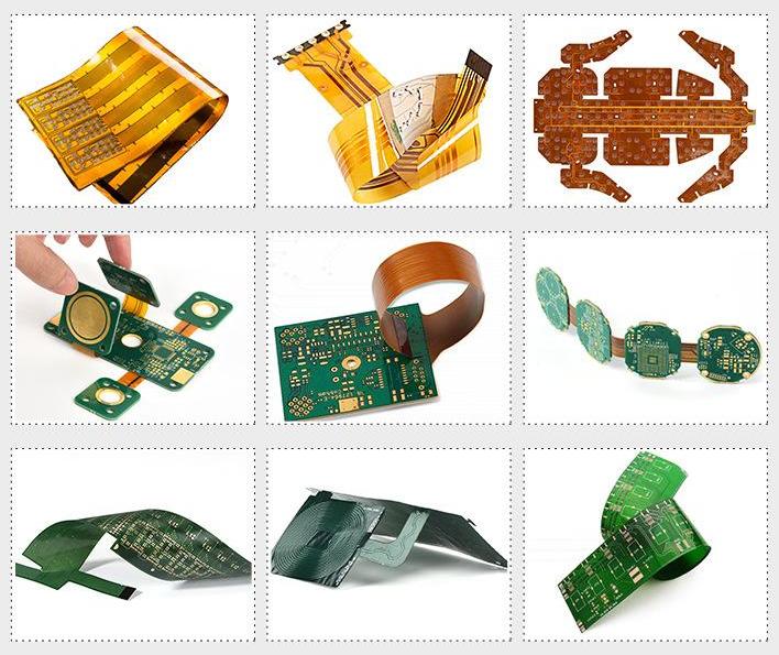
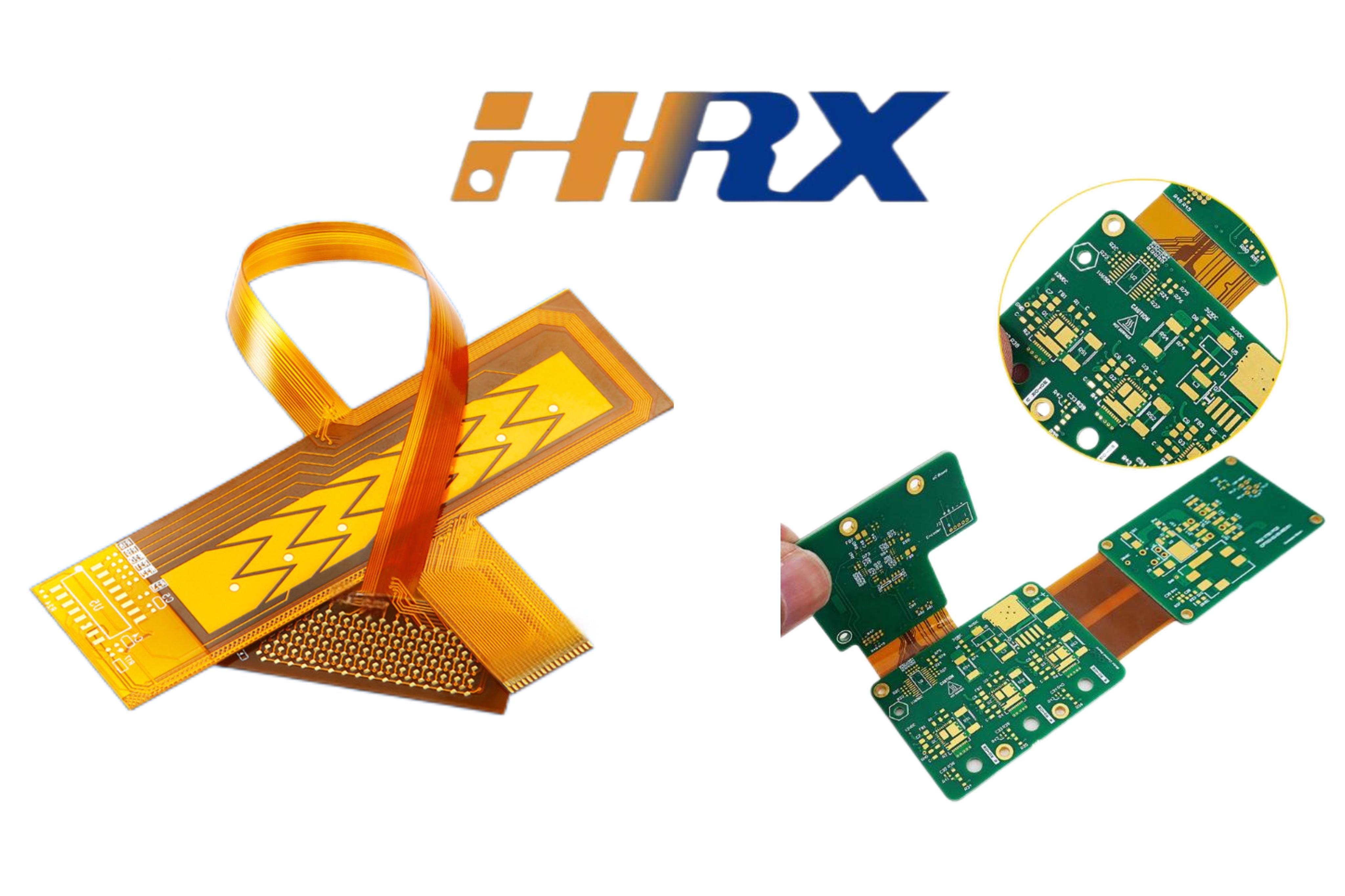
Shenzhen Huaruixin Electronics Co., Ltd. is a highly professional manufacturer specializing in the design and production of FPC&PCB&Rigid - Flex Printed Board. We wholeheartedly welcome new and old friends to engage in technical exchanges and collaborative learning, aiming to jointly promote the development and innovation of the printed circuit board industry.

Let’s talk! We’ll provide the perfect solution for you!
-
 Huaruixin Electronics mainly produces printed circuit boards as the core business, to provide customers with one-stop solutions for FPC/PCB production, components sourcing and Assembly.
 - WHAT WE DO — PCB Design Solutions — Flex PCB Production — Components Sourcing — FPC&PCB Assembly
- PRODUCTS — Single Sided Flexible Circuits — Double Sided Flexible Circuits — Multilayer Flexible Cirucits — Rigid-Flex Circuits — FPC Assembly — PCB Assembly
- CAPABILITY — FPC Capability — Rigid-Flex Capability — PCB Capability — Assembly Capability
- Copyright © 2024 Shenzhen Huaruixin Electronics Co., Ltd. All Rights Reserved.
- Design By BONTOP


