
Search


The Manufacturing Process of FPC Flexible Circuit Boards
- Mar 06,2025
-
Share
Flexible Printed Circuit (FPC) boards, as the cornerstone of modern electronics, are lauded for their remarkable flexibility, ultra - thin form factor, and high - density interconnection capabilities. These attributes render FPC boards indispensable in a wide gamut of applications, from the sleek designs of smartphones to the intricate circuitry of aerospace systems. The manufacturing process of FPC boards is a highly intricate and precise sequence of operations, with each step playing a pivotal role in determining the quality, reliability, and functionality of the final product. Shenzhen Huaruixin Electronics Co., Ltd., a trailblazer in the FPC production domain, adheres to a scrupulously refined manufacturing process to consistently deliver top - tier FPC boards that meet the most stringent industry standards.
1. Material Preparation
Substrate Selection
The initial and crucial step in FPC manufacturing is the astute selection of the flexible substrate. In the FPC industry, Polyimide (PI) and polyester (PET) stand out as the two most prevalently used materials. PI substrates are renowned for their exceptional heat resistance, chemical inertness, and robust mechanical strength. These properties make them the material of choice for applications in harsh environments, such as automotive under - hood electronics and high - altitude aerospace components, where resistance to extreme temperatures and chemical exposure is essential. PET substrates, on the other hand, offer a more cost - effective alternative with commendable flexibility. They are commonly employed in less demanding consumer electronics, like wearable devices and low - end mobile accessories, where cost - efficiency and basic flexibility requirements are prioritized. The thickness of the substrate, a critical parameter, typically spans from 12.5μm to 125μm. This range allows for customization based on the specific requirements of the FPC design, such as the need for enhanced flexibility in highly bendable applications or increased mechanical stability in more rugged environments.
Copper Foil Lamination
Subsequent to substrate selection, the process of copper foil lamination comes into play. The copper foil, which serves as the primary conductor for electrical signals in FPC boards, is laminated onto the chosen substrate. There are two main variants of copper foils: electrodeposited (ED) copper foil and rolled - annealed (RA) copper foil. ED copper foil, characterized by its relatively rough surface morphology, provides enhanced adhesion to the substrate. This roughness creates a larger contact area between the copper foil and the substrate, ensuring a more secure bond. However, this rough surface may also introduce a certain degree of electrical resistance, which can impact the performance of high - speed or low - resistance - sensitive circuits. In contrast, RA copper foil boasts a smoother surface, resulting in lower electrical resistance. This makes it ideal for applications where minimizing signal attenuation and maximizing electrical conductivity are crucial, such as in high - frequency communication modules. Nevertheless, the smoother surface of RA copper foil requires more meticulous lamination techniques to ensure a strong and reliable adhesion. The lamination process is executed using high - pressure and high - temperature laminators. The temperature and pressure are precisely calibrated and controlled to ensure a tenacious bond between the copper foil and the substrate. This precise control is essential to prevent delamination, which can lead to electrical failures and reduced product lifespan.
2. Circuit Pattern Formation
Photolithography
Photolithography represents a linchpin in the creation of intricate circuit patterns on FPC boards. This process begins with the uniform application of a photoresist onto the copper - clad substrate. The photoresist can be of either the liquid - based type, applied through techniques such as spin - coating or spray - coating, or the dry - film type. Each type has its own advantages and is selected based on factors such as the complexity of the circuit pattern, production volume, and cost considerations. After application, the substrate is subjected to a baking process. This baking step serves to harden the photoresist, ensuring its integrity during the subsequent exposure and development stages. Subsequently, a photomask, which contains the exact circuit pattern to be transferred, is carefully aligned and placed over the coated substrate. Ultraviolet (UV) light is then projected through the photomask. The regions of the photoresist exposed to the UV light undergo a chemical transformation, either cross - linking (in the case of negative photoresist) or decomposition (in the case of positive photoresist). The areas shielded by the photomask remain unaltered. This differential response to UV light forms the basis for pattern transfer in photolithography.
Development
Following the exposure step, the substrate enters the development phase. In this stage, a developer solution is used to selectively dissolve either the unexposed regions (in the case of positive photoresist) or the exposed regions (in the case of negative photoresist) of the photoresist. This dissolution process leaves behind a precise replica of the photoresist pattern that corresponds exactly to the circuit pattern on the photomask. The development time and the concentration of the developer solution are carefully optimized and tightly controlled. Deviations in these parameters can lead to issues such as under - development, where residual photoresist remains, or over - development, which can cause the loss of fine - line features and inaccurate pattern transfer.
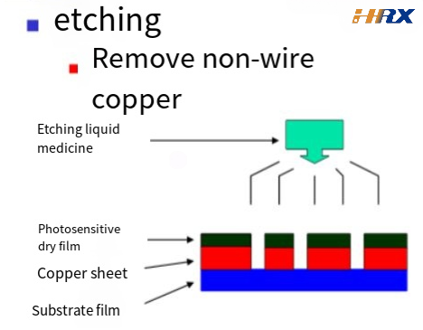
Etching
Once the photoresist pattern is firmly established, the etching process commences. An etchant, such as ferric chloride or a mixture of sulfuric acid and hydrogen peroxide, is introduced to selectively dissolve the unprotected copper areas. The etching rate is influenced by a multitude of factors, including the etchant concentration, temperature, and agitation. Precise control of these variables is of utmost importance to ensure uniform copper etching across the entire substrate. Uneven etching can result in issues such as line width variations, short circuits, or open circuits, all of which can severely compromise the functionality of the FPC board. After the etching process is complete, the residual photoresist is removed using a stripping solution. This stripping step is crucial to prepare the board for subsequent processing steps.
3. Hole Formation
Drilling
For FPC boards that require vias (holes for establishing electrical connection between different layers), drilling is an essential operation. Laser drilling has emerged as a dominant method in FPC manufacturing due to its unrivaled precision and ability to create micro - diameter holes with high aspect ratios. The laser beam, focused to a fine point, vaporizes the substrate and copper foil in a highly controlled manner to form the holes. The size, location, and depth of the holes are meticulously controlled by the laser drilling equipment. Parameters such as laser power, pulse duration, and number of pulses are carefully adjusted according to the thickness of the substrate and the desired hole diameter. This precise control is crucial to ensure the integrity of the vias and their proper functioning in facilitating electrical connection between different layers of the FPC board.
Plating
Subsequent to drilling, the holes must be plated with copper to render them electrically conductive. The plating process involves immersing the FPC board in a copper - plating solution. Through an electrochemical reaction, copper ions in the solution are deposited onto the walls of the holes and the surface of the board. The plating thickness is closely monitored and controlled to ensure optimal electrical connectivity. A thin initial layer of copper is typically deposited first to provide a uniform seed layer, followed by a thicker layer to meet the specific electrical conductivity requirements of the application. Precise control of the plating thickness is essential to prevent issues such as insufficient conductivity due to thin plating or short circuits due to excessive plating.
4. Surface Treatment
Soldermask Application
A soldermask is applied to the FPC board to safeguard the circuit traces from oxidation, mechanical damage, and to prevent solder bridges during the assembly process. The soldermask can be either a liquid - based or a dry - film material. Liquid - based soldermasks are often applied using screen - printing techniques, which offer good flexibility in terms of pattern customization. Dry - film soldermasks, on the other hand, are laminated onto the board and are known for their high - resolution printing capabilities. The soldermask features precisely designed openings at the pads where components will be soldered. These openings, also known as solder windows, are critical for ensuring proper solder wetting and reliable component attachment. The curing process of the soldermask, which can be achieved using heat or UV light depending on the type of soldermask material, is carefully controlled to ensure the soldermask's durability and adhesion.
Surface Finish
There is a diverse range of options for the surface finish of FPC boards, each catering to specific application requirements. One widely adopted surface finish is electroless nickel immersion gold (ENIG). In this process, a layer of nickel is deposited on the copper surface through an electroless plating method. This nickel layer provides a barrier against copper diffusion and corrosion. Subsequently, an immersion gold layer is applied on top of the nickel layer. The gold layer offers excellent solderability and corrosion resistance, making it suitable for applications where reliable soldering and long - term environmental protection are crucial. Another popular alternative is organic solderability preservative (OSP). OSP involves applying an organic coating to the copper surface. This coating forms a thin, protective layer that prevents oxidation and enhances solderability. The choice of surface finish is highly dependent on factors such as the application environment, cost considerations, and the required solderability performance.
5. Testing and Inspection
Electrical Testing
Prior to the shipment of FPC boards, comprehensive electrical testing is carried out to ensure their proper functionality. This testing regimen encompasses continuity testing, which is used to detect open circuits in the circuit traces. Insulation resistance testing is also performed to verify the absence of short circuits between different conductors. Additionally, impedance testing is conducted to ensure that the electrical impedance of the circuit traces meets the design specifications. This is particularly important in high - speed applications, where impedance mismatches can lead to signal reflections and degradation. Automated test equipment, such as flying - probe testers and in - circuit testers, are commonly used to execute these tests with high efficiency and accuracy. These testers can quickly and precisely measure electrical parameters and identify any defects in the FPC boards.
Visual Inspection
Visual inspection also forms an integral part of the quality control process. Trained operators conduct a meticulous visual examination of the FPC boards for any visible defects, including missing traces, short circuits, improper soldermask coverage, or damaged holes. High - magnification microscopes may be used to detect minute defects that are not visible to the naked eye. In addition, X - ray inspection can be employed to assess the integrity of the vias and the internal layers of multi - layer FPC boards. X - ray inspection allows for the detection of hidden defects, such as voids in the vias or misalignment of internal layers, which can significantly impact the performance and reliability of the FPC board.
In conclusion, the manufacturing process of FPC flexible circuit boards is a highly sophisticated and exacting endeavor. Each step, from the initial material selection to the final testing and inspection, is critical in determining the quality, performance, and reliability of the FPC boards. Shenzhen Huaruixin Electronics Co., Ltd. continues to invest in state - of - the - art equipment, advanced manufacturing technologies, and highly skilled personnel to optimize this process and deliver top - tier FPC products that meet the ever - evolving and diverse demands of the electronics industry.

Let’s talk! We’ll provide the perfect solution for you!
-
 Huaruixin Electronics mainly produces printed circuit boards as the core business, to provide customers with one-stop solutions for FPC/PCB production, components sourcing and Assembly.
 - WHAT WE DO — PCB Design Solutions — Flex PCB Production — Components Sourcing — FPC&PCB Assembly
- PRODUCTS — Single Sided Flexible Circuits — Double Sided Flexible Circuits — Multilayer Flexible Cirucits — Rigid-Flex Circuits — FPC Assembly — PCB Assembly
- CAPABILITY — FPC Capability — Rigid-Flex Capability — PCB Capability — Assembly Capability
- Copyright © 2024 Shenzhen Huaruixin Electronics Co., Ltd. All Rights Reserved.
- Design By BONTOP