Miniaturization and High-Density Wiring of FPCs in Smart Watches: Production Process Requirements and Implementation Methods
- Dec 23,2024
-
Share
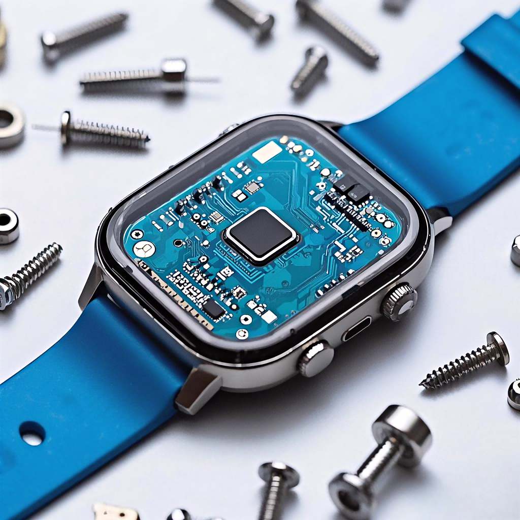
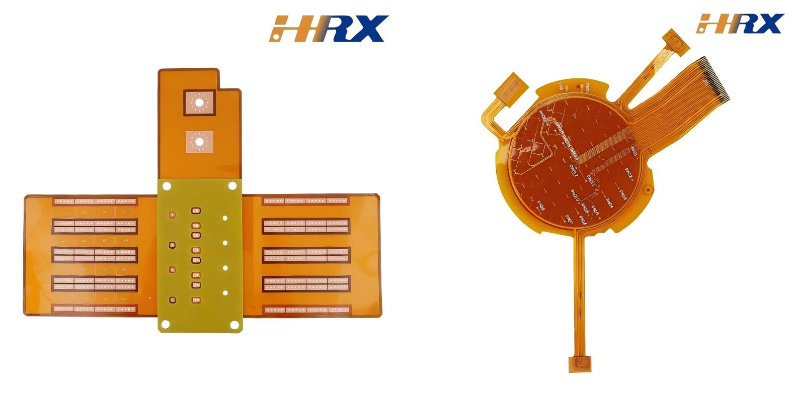
In the era of wearable technology, smart watches have witnessed a remarkable surge in popularity. The Flexible Printed Circuits (FPCs) deployed within smart watches serve as the linchpin in interconnecting a diverse array of components, including the power source (battery), the central processing unit (main control chip), sensors of various modalities, and the visual display interface (display screen). The exigencies of compact form factor and enhanced functionality have rendered miniaturization and high-density wiring of FPCs not merely an advantage but an absolute necessity to satiate the stringent design prerequisites of modern smart watches.

I. Specific Implementation Methods of Miniaturization and High-Density Wiring of FPCs in Smart Watches
Component Selection
Small-Size Chip Adoption: The preference gravitates towards highly integrated and diminutively packaged semiconductor chips. For instance, the Nordic nrf52832-qfaa chip, which houses a Cortex - M4 core and an integrated Bluetooth transceiver, along with Low Dropout (LDO) regulators sporting DFN4 packages. These chips, by virtue of their compact footprint, substantially curtail the spatial occupancy of the circuit board substrate.
Miniature Passive Component Utilization: Capacitors, resistors, and other passive elements with even smaller form factors, such as those conforming to 0201 and 01005 package standards, are judiciously selected. This strategic choice augments the packing density of components, thereby facilitating a concomitant increase in the wiring intricacy and density within the confined spatial envelope.
Circuit Design
Layout Optimization: The layout and physical conformation of the FPC are meticulously engineered, taking into account the internal geometry and the spatial disposition of each constituent component of the smart watch. The FPC is artfully contoured to snugly conform to the internal contours, perhaps following the curved periphery of the watch casing, thereby optimizing the utilization of the scarce available space.
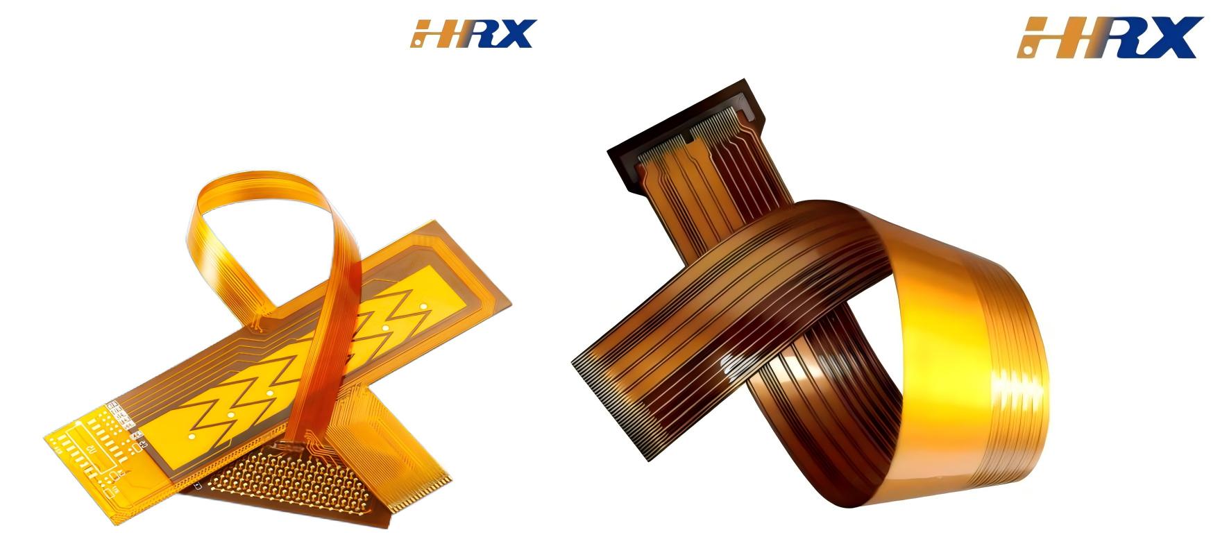
Multi-Layer Wiring Design: A multi-layered FPC architecture is implemented. By augmenting the number of wiring strata and segregating distinct classes of electrical conductors, such as power distribution lines and signal transmission paths, onto separate layers, the incidence of crosstalk and mutual interference is mitigated. This stratagem not only bolsters the wiring density but also enables a more elaborate and comprehensive network of electrical interconnections.
Reduced Line Spacing: Within the ambit of conforming to established electrical performance benchmarks and safety norms, the inter-line spacing and the width of individual conductors are minimized to the greatest extent practicable. This optimization maneuver augments the count of wiring traces per unit area. However, scrupulous attention must be paid to preclude the occurrence of short circuits. State-of-the-art high-precision etching methodologies are requisitely employed to safeguard the dimensional accuracy and integrity of the etched lines.
Manufacturing Process
High-Precision Etching: Given the minuscule line spacing and narrow conductor widths, the parameters governing the etching process, including the concentration of the etching solution, the duration of etching, and the temperature regime, demand precise calibration and control. For instance, single-panel precision etching techniques are frequently resorted to, wherein the aqua control system and associated paraphernalia are harnessed to maintain the concentration of the etching solution within an exquisitely narrow tolerance band.
Laser Drilling: Laser drilling technology is enlisted to fabricate vias of diminutive diameter, thereby enhancing the via density. The high positional accuracy and repeatability of the laser drilling process confer a distinct advantage in augmenting the flexibility and density of inter-layer wiring connections, while simultaneously safeguarding the mechanical robustness of the FPC laminate.
Surface Mount Technology: Advanced surface mount assembly techniques are deployed to effectuate the precise and efficient attachment of minuscule electronic components onto the FPC substrate. This technological paradigm not only augments the packing density and throughput of the assembly process but also vouchsafes the reliability and stability of the component-to-board electrical interfaces.
II. Special Requirements of Miniaturization and High-Density Wiring of Smart Watch FPCs for the Production Process
Circuit Line Fabrication
High-Precision Etching: As previously alluded to, the etching parameters wield a decisive influence over the quality of the fabricated circuitry. Even a marginal deviation in the concentration of the etching solution, the etching time, or the temperature can precipitate non-uniform line widths, open circuits, or short circuits, any of which are anathema to the achievement of high-density wiring fidelity.
Laser Drilling: The precision and density of laser-drilled vias are of primordial importance. The vias must possess both a small diameter and high positional accuracy to ensure seamless signal transmission between layers, while simultaneously upholding the mechanical integrity and load-bearing capacity of the FPC laminate.
Micro-Component Mounting: High-precision pick-and-place machines, endowed with micron-level placement accuracy, are indispensable for the accurate emplacement of ultra-small components, such as those adhering to 0201 and 01005 package specifications. The placement tolerances are stringently defined to preclude the occurrence of short circuits and to ensure the integrity of electrical connections.
Anti-Solder Bridging Process: Owing to the diminutive pitch of the surface mount pads, the parameters of the soldering process, including the solder paste composition, reflow temperature profile, and soldering time, must be painstakingly optimized. Additionally, the selection of an appropriate solder alloy, with favorable wetting and spreading characteristics, is of paramount significance. Optical inspection mechanisms, such as Automated Optical Inspection (AOI) and X-ray inspection, are deployed at multiple junctures, including post-solder paste printing, post-component placement, and post-soldering, to detect and expunge solder bridging defects and other anomalies in a timely fashion.
Lamination and Film Pressing
Vacuum Lamination Technology: Vacuum lamination technology is harnessed to effectuate a seamless and void-free bond between the single-panel substrate and the dry film. This technological innovation obviates the foibles associated with traditional roller-type dry film laminators, such as non-uniform rolling pressure, inadequate dry film degassing, uneven heating, and suboptimal adhesion. The elimination of bubbles between the dry film and the copper conductor layer serves to enhance the yield and quality of the circuit fabrication process.
Reliable Lamination Process: During the lamination process, each layer of the FPC laminate must be bonded with tenacity and uniformity, devoid of any voids, delamination, or other structural imperfections. Stringent control of lamination pressure, temperature, and time, in conjunction with the selection of premium-grade adhesives, is essential to ensure the structural integrity and long-term reliability of the FPC laminate.
Inspection Stage
Optical Inspection: Automated Optical Inspection (AOI) and X-ray inspection modalities are deployed as part of a comprehensive inspection regimen. These inspections are conducted at multiple critical junctures in the production process, including after solder paste printing, after component placement, and after soldering. The inspections are designed to detect a gamut of defects, such as short circuits, open circuits, incomplete etching, pinholes, misaligned components, and solder bridging, thereby ensuring the conformance of the FPC to the requisite quality and performance standards.
Electrical Performance Testing: A battery of comprehensive electrical performance tests is mandatorily administered. These tests encompass insulation resistance testing, dielectric withstand voltage testing, and signal transmission testing. The insulation resistance test ascertains the adequacy of the FPC's insulating properties, the dielectric withstand voltage test verifies the FPC's ability to withstand applied voltages without breakdown, and the signal transmission test validates the fidelity and integrity of signal propagation across the FPC circuitry.
Shenzhen Huaruixin Electronics Co., Ltd., a preeminent professional entity in the domain of FPC manufacturing and sales, replete with a wealth of experience and technological acumen, extends a warm and cordial invitation to both existing and prospective clients to engage in a collaborative dialogue and knowledge-sharing endeavor. We are poised to offer bespoke solutions and insights that cater to the evolving exigencies of the smart watch and wearable technology sectors.


 Huaruixin Electronics mainly produces printed circuit boards as the core business, to provide customers with one-stop solutions for FPC/PCB production, components sourcing and Assembly.

